p-n junctions
A very good video on this can be found at: How a pn junction diode works
Band Theory
As we learnt in the waves section of the course, spectra, individual atoms have fixed energy levels for their electrons. When the atoms combine in solids there is a mixing of energy levels to form two bands which then determines the electrical conductivity of the material.
Solids can either freely conduct electricity, not conduct electricity or as was discovered last century be able to conduct electricity under certain circumstances. These latter materials are called semi-conductors.
To explain these properties the band theory of conduction was developed. This theory has two bands where electrons can exist. Each material has its own characteristic band structure.
The valence band is the one in which electrons are in orbitals which are associated with atoms and therefore unable to move through the solid.
The conduction band where electrons are not associted with individual atoms, but are free to move throughout the solid because there are empty available energy levels.
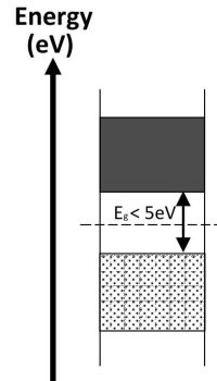
Where the conduction band and valence band overlap the material is a conductor of electricity. Where there is a small energy gap between the conduction and valence bands the material is a semi-conductor and will only conduct when valence electrons have been given sufficient energy to cross the energy gap. If the gap between the valence and conductions bands is large the material is classed as an insulator and will not normally conduct electricity.
Some metals have free electrons and partially filled valence bands, therefore they are highly conductive. Some metals have overlapping valence and conduction bands. Each band is partially filled and therefore they are conductive.
| Conductor | Insulator | Semi-conductor |
|---|---|---|
| Valence band is full and there are free electrons in the conduction band because it overlaps with the valence band. These electrons are free to move throughout the material. | All electrons are contained the valence band and there are none in the conduction band. Electrons in the full valence band do not have enough energy to cross the large gap and so the material does not conduct electricity. | At cold temperature all of the electrons are contained in the valence band. With high enough temperature some electrons can be promoted to the conduction band leaving holes in the valence band, which allows cunduction of electricity. The higher the temperature the greater the conduction. |
Upper band = conduction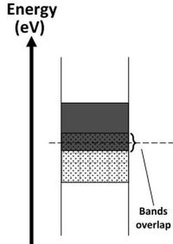 |
Lower band = valence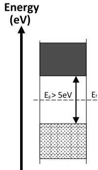 |
 |
Doping
Semi-conductor materials tend to be based on the element silicon. Silicon has 4 outer electrons in its outermost electron shell. Each of these 4 electrons bond with electrons from 4 other atoms to form covalent bonds holding the silicon together. This means that none of the outer shell electrons are in the conduction band. They are all in the valence band. At room temperature it is possible to give some of the electrons involved in bonding sufficient energy to jump into the conduction band. These electrons (and the holes they leave behind) are able to move and so a flow of charge can occur. This is electrical conduction. The videos above show how this occurs.
To enhance the number of electrons in the conduction band or the number of holes in the valence band silicon can be doped with small amounts of group 13 or group 15 elements.
When using a group 13 element such as gallium, they have only got 3 outer electrons. This means that when the gallium bonds with silicon it is only able to make 3 bonds instead of 4. Silicon is left with an unpaired electron which is ready to bond. The gallium has introduced a hole into the valence band of the solid. An electron from a neighbouring atom can jump into this hole and so the hole moves through the material. This is similar to the flow of positive charge, and so it is possible to have a positive current. This type of doping is called p-type
When using a group 15 element such as arsenic, they have 5 outer electrons. This means that when arsenic bonds with silicon 4 electrons are used to bond with the silicon and the fifth electron is left over. This electron goes into the conduction band of the solid and increases the conductivity of the material by the flow of negative charge by these electrons. This type of material is called an n-type.
p-n Junction
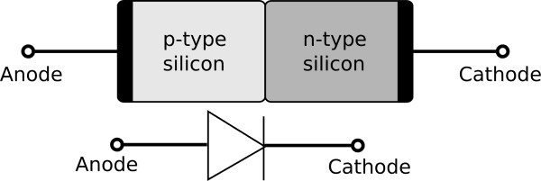
When an n-type doped semi-conductor is placed in contact with a p-type semi-conductor a special region is formed which is a p-n junction. This area has specific electrical properties which are described and modelled in the videos referenced above.
The structure and symbol for a p-n junction diode is given below.
Depletion layer
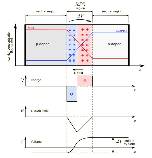
When the p-n junction is formed electrons in the conduction band of the n-type move into the conduction band of the p-type and then combine with holes. Holes in the valence band of the p-type move into the valence band of the n-type and combine with electrons. The result is that the region where the two materials are joined becomes depleted in both positive and negative charge carriers.
An electric filed is setup in the depletion zone because of the charges in the two zones. Remember that originally both n-type and p-type materials are electrically neutral. As the n-type donates electrons to the p-type the remaining region develops a net positive charge. The p-type which was neutral gains electrons and becomes negatively charged in the region of the junction.
The following graphic illustrates the potential field that is set up, and where the neutral regions remain.
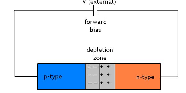
Forward Bias
For any further current to travel through the region an external electric field must be applied for electrons and holes to overcome the repulsions of the field setup by the depletion layer. Notice that in the diagram above the cell is connected in a forward bias orientation. The positive pole of the cell is attached to the p-type semiconductor, and the negative pole of the cell to the n-type semiconductor. Providing there is sufficient energy supplied by the external field current will be able to pass through the diode.
In Forward bias the electric field of the depeltion zone is reduced.
Reverse Bias
In a reverse bias situation the depletion layer gets larger and it becomes even more difficult for current to pass through the material. In reverse bias the p-n junction behaves as if it were an insulator. This menas that p-n juntions behave as diodes, only allowing current to flow in a single direction.
In reverse bias the electric field of the depletion zone is increased.
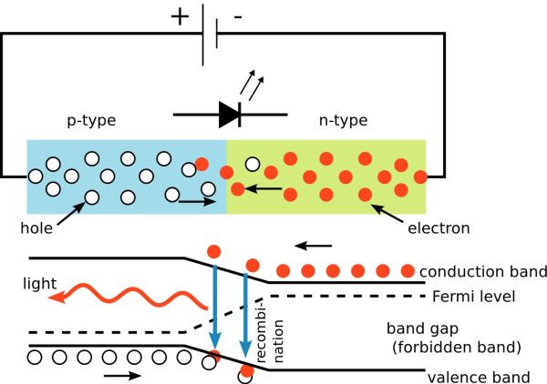
Light Emitting Diodes
In some materials the recombination of an electron from the conduction band of the n-type with a hole in the valnce band of the p-type produces a specific frequency of light. This only occurs when in the forward bias mode because current must be passing for the process to continue making light. The light produced can be in the visible region and so these devices are called light emitting diodes (LED's for short).
The forward bias potential difference across the junction causes electrons to move from the conduction band of the n-type semiconductor towards the conduction band of the p-type semiconductor. Photons are emitted when electrons 'fall' from the conduction band into the valence band either side of the junction. This is at a fixed frequency because of the specific energy gap between the conduction band and valence bands. This has allowed us to fine tune the manufacture of LEDs to produce different colours of the spectrum as well as white light.
Solar Cells
Imagine a diode where light is taken in and this is used to separate a hole from an electron because the light is of the correct frequency to cause this promotion. This will increase the number of charge carriers in the material. Effectively the opposite of the LED is a very useful device called a photovoltaic cell. These are cells capable of taking sunlight and directly converting it into electrical energy.

The amount of electricity the international space station can generate using its solar cells is 120 kilowatts - enough to power 40 homes. Normally it generates between 75 to 90 killowatts of electrical energy.
The absorption of photons provides energy to 'raise' electrons from the valence band of the semiconductor to the conduction band. The p-n junction causes the electrons in the conduction band to move towards the n-type semiconductor and a potential difference is produced across the solar cell. This can then provide a current to an external circuit.
Another very good video on pn junctions, showing the operation of a solar cell: The pn juntion - how a solar cell works